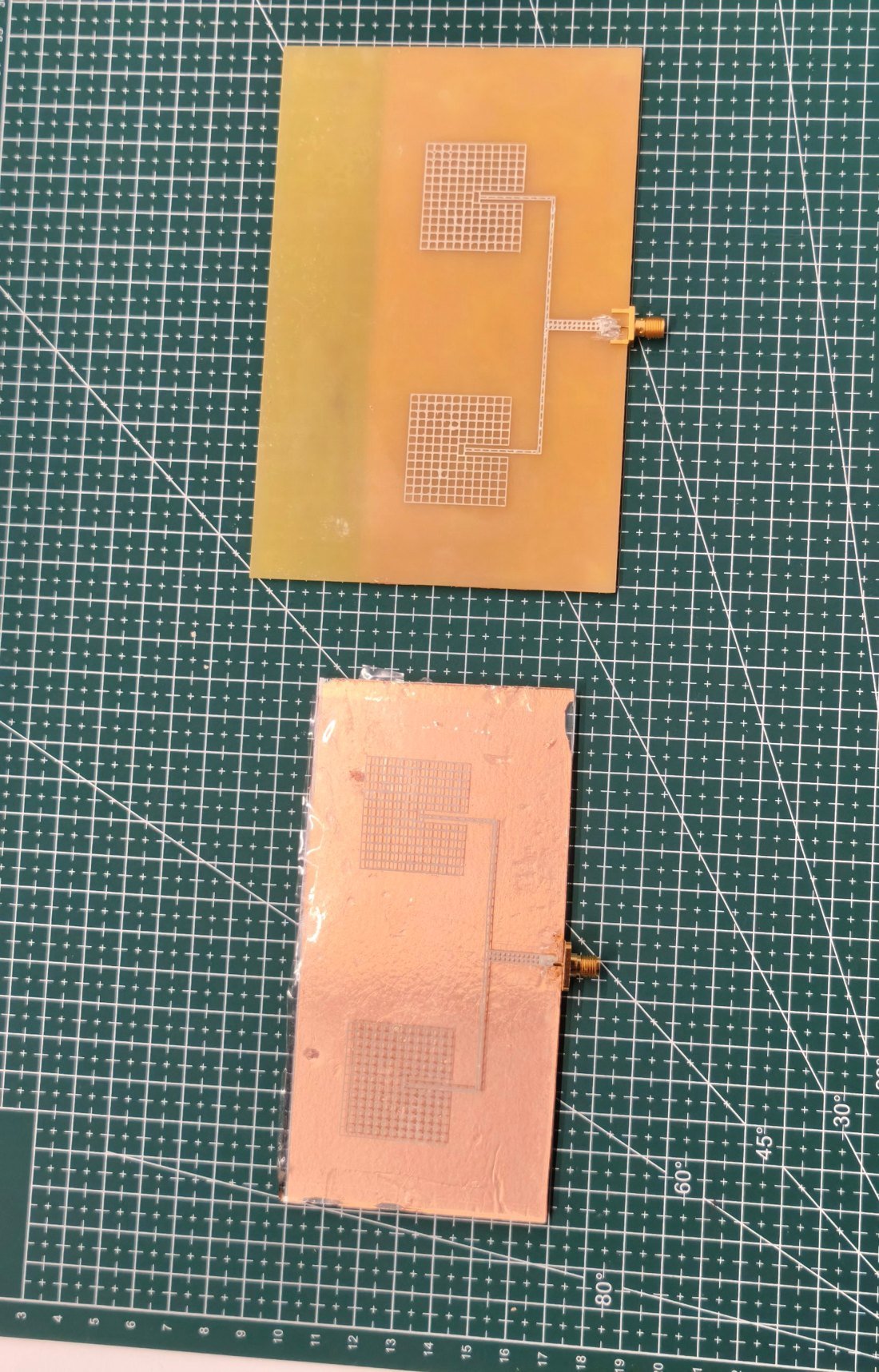
FR4
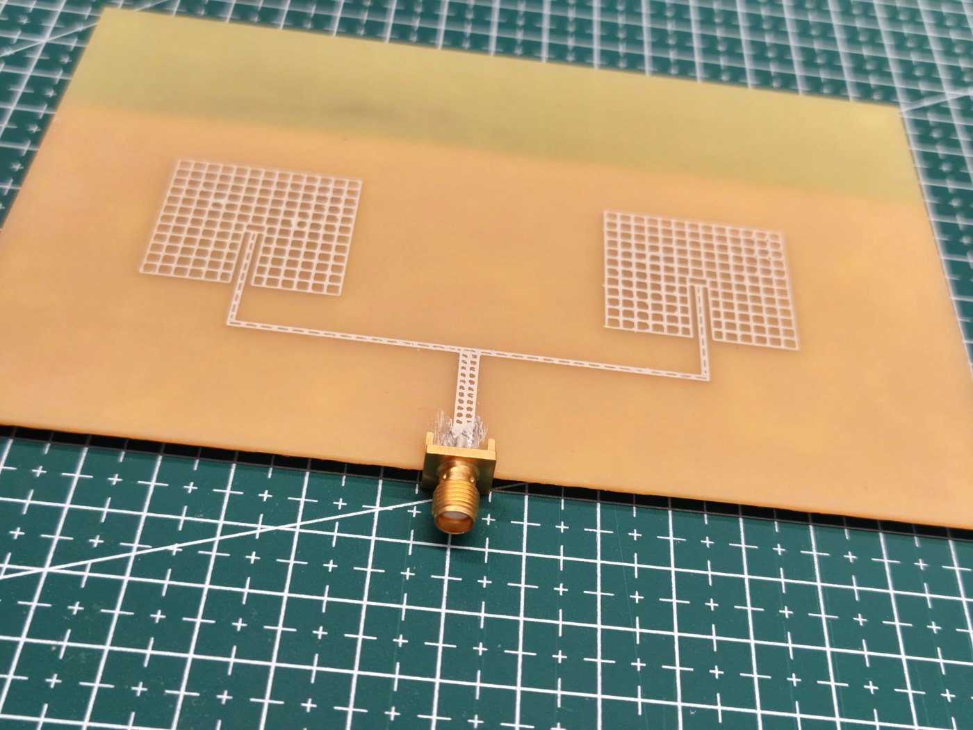
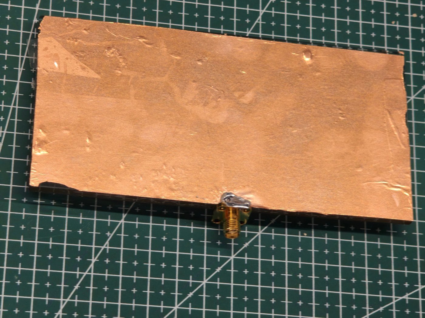
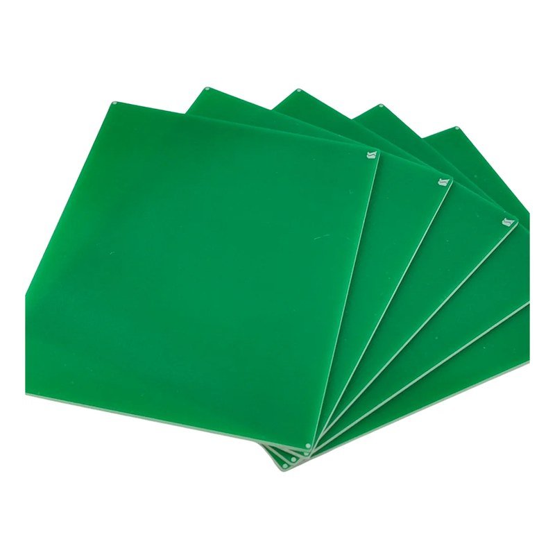
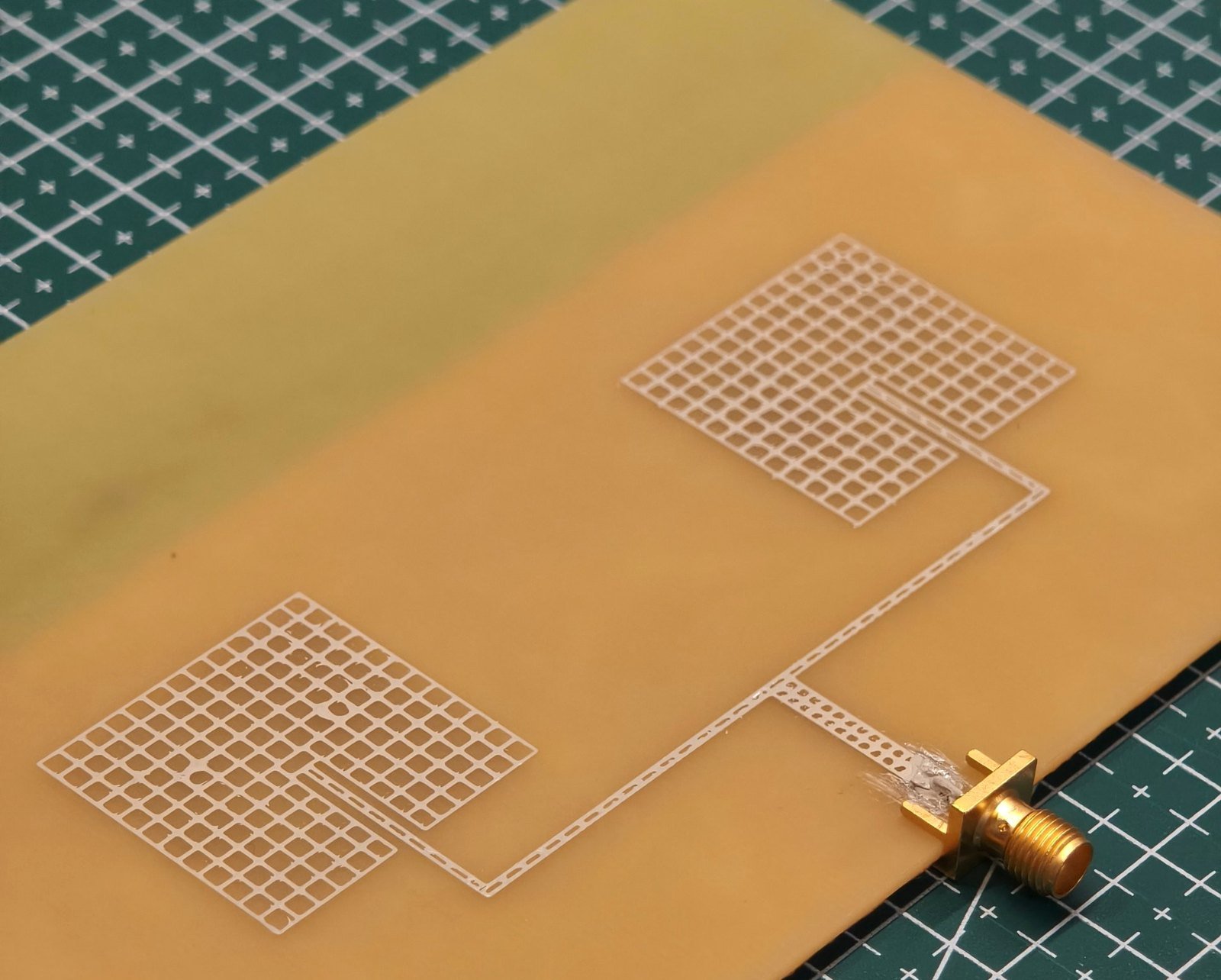
Printed directly on FR4, a mechanically stable substrate widely used in rigid circuits. Copper tape covers the reverse side as a conductive backing.
- Substrate
- FR4
- Support
- None
- Backing
- Copper tape
- RF connection
- SMA
Two prototypes with the same antenna geometry were printed with Monobee: one on FR4, the other on PET that was then bonded to glass. Both were backed with copper tape and connected to a vector network analyzer (VNA) for RF reflection measurements.
Initial measurements showed distinct input reflection responses, with pronounced S11 minima at different frequencies for the two configurations.
RF antenna development depends on conductive geometry, substrate properties and the surrounding dielectric structure. Even when the conductive layout stays the same, changing the substrate configuration can shift input impedance and frequency response.
The goal was not to build a complete wireless product, but to investigate the fabrication and preliminary RF behavior of printed antennas on two substrate configurations.
Both prototypes share the same nominal layout: two mesh patch regions connected to a common feed. Keeping the printed geometry constant makes it possible to see how the underlying material stack changes the measured RF response.
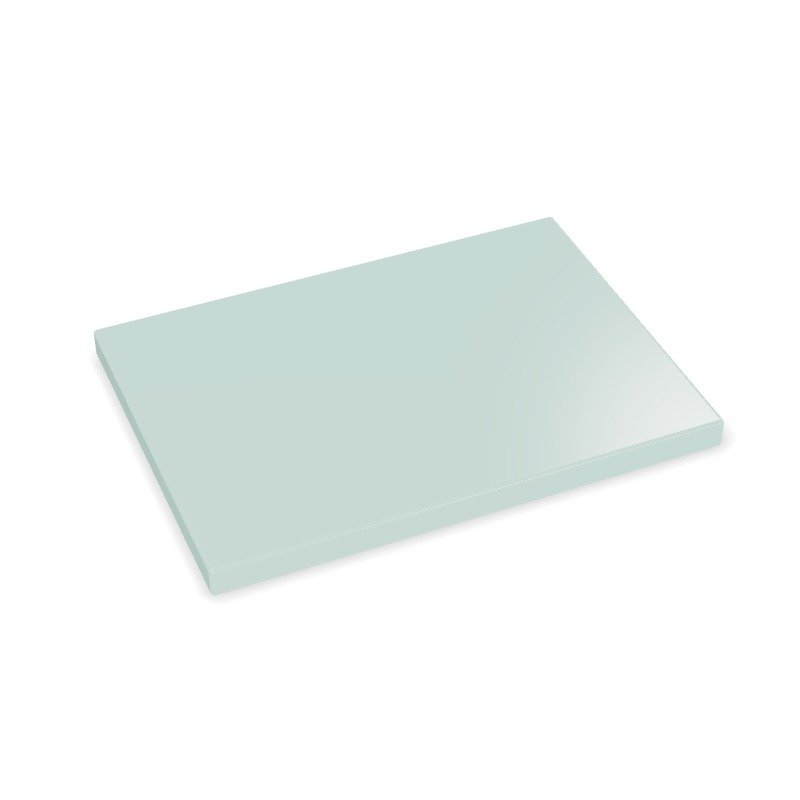
Printed directly on FR4, a mechanically stable substrate widely used in rigid circuits. Copper tape covers the reverse side as a conductive backing.
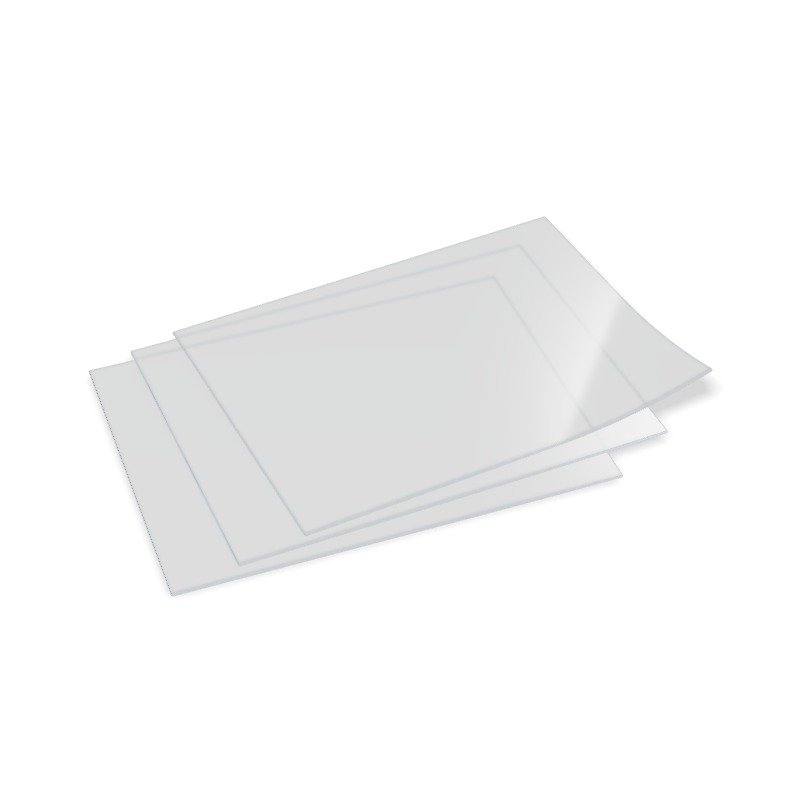
Printed on flexible PET, then bonded to a glass support with care taken to avoid air gaps. Copper tape covers the back of the assembly.
An antenna is the conductor, the substrate, the backing and the feed working together.
Differences in dielectric properties, thickness and layer arrangement influence input impedance and frequency response. Printing the same design on two stacks lets researchers study these effects by direct comparison.
Both patterns were printed from the same digital geometry with Direct Ink Writing, then built into their test assemblies.
| PARAMETER | FR4 | PET ON GLASS |
|---|---|---|
| Fabrication | Direct Ink Writing | Direct Ink Writing |
| Printed design | RF antenna pattern | Same nominal pattern |
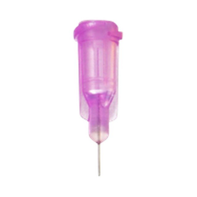
| Tip | 30G metal, 0.16 mm ID | 30G metal, 0.16 mm ID |
| Substrate | FR4 | PET |
| Additional support | None | Glass |
| Backing | Copper tape | Copper tape |
| RF connection | SMA | SMA |
| Characterization | VNA, S11 | VNA, S11 |
S11 is the input reflection measured at the antenna port. Shown in decibels, a more negative value means less power is reflected at that frequency, so a pronounced minimum points to a region of better impedance matching.
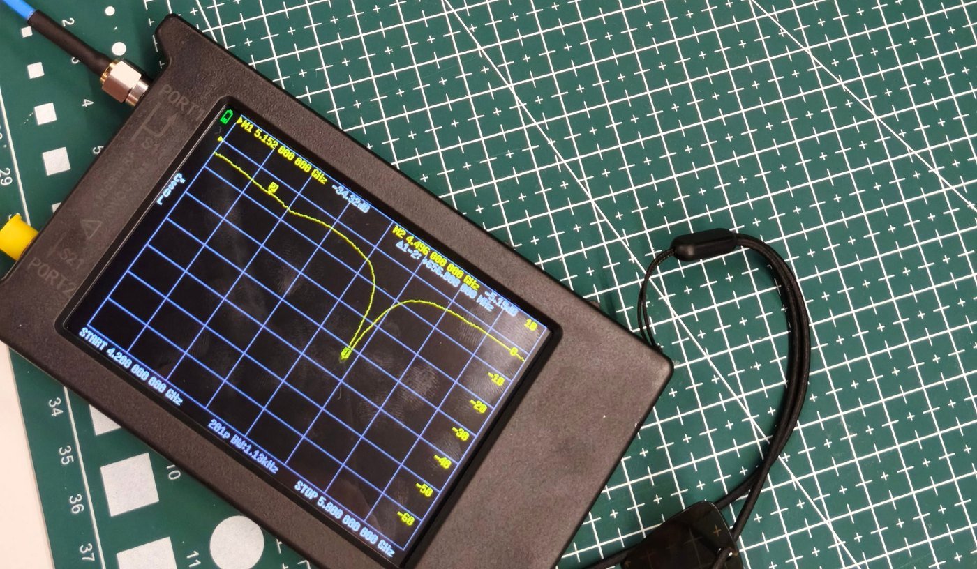
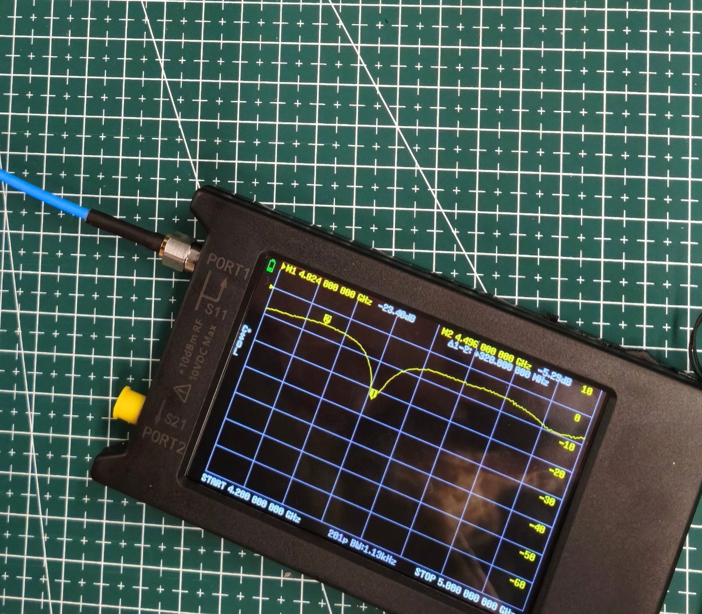
Both prototypes were measured with a handheld VNA over the same 4.2 to 5.8 GHz sweep.
A deep, narrow reflection minimum near 5.152 GHz, indicating reduced input reflection around that frequency in the tested configuration.
The minimum appears at a lower frequency than on FR4, despite the shared nominal antenna geometry.
The shift in the S11 minimum is consistent with antenna behavior depending on its material and structural environment. It cannot be attributed to the substrate alone without controlling backing geometry, layer thickness, feed connections and calibration, so these results are a preliminary comparison rather than a full electromagnetic characterization.
Values are read from the VNA screen during measurement and are preliminary. Calibration details, raw exports and repeatability have not yet been independently verified. S11 alone does not establish gain, radiation efficiency or wireless performance.
The substrate is part of the antenna design.
A printed antenna is not defined by its conductive geometry alone. Its electrical behavior also depends on the dielectric materials, conductive backing and feed arrangement, which is why the same pattern produced different S11 responses on FR4 and on PET bonded to glass.
Direct Ink Writing deposits conductive structures straight from a digital design onto suitable substrates, with no masks, etching or outsourced fabrication runs. That makes each antenna iteration faster and more cost-efficient to produce: change the geometry or the material stack, print it in-house and take it straight to RF characterization.
Printed RF structures are relevant well beyond this comparison.
These are potential applications of printed RF structures. This study is a preliminary reflection characterization, not a demonstration of a complete wireless device.
The same nominal antenna, printed on FR4 and on PET bonded to glass, showed S11 minima near 5.152 GHz and 4.824 GHz. Combining digital pattern fabrication with RF characterization lets researchers treat antenna geometry and substrate configuration as connected design variables.
RELATED MATERIALS: SILVER CONDUCTIVE INKS →Yes. Monobee deposits conductive materials along digitally defined patterns, so experimental antenna geometries can be fabricated in-house.