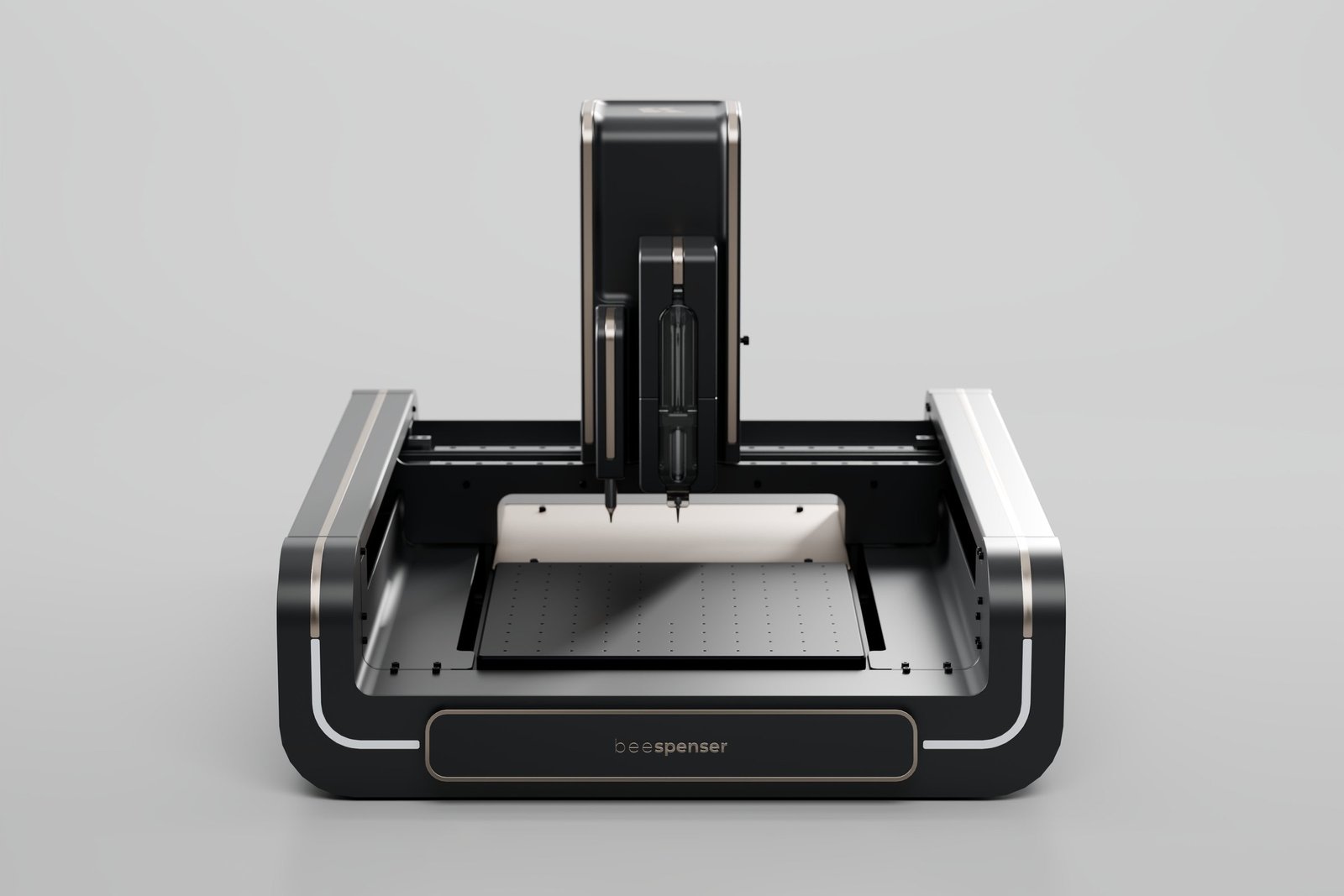
MONOBEE · MICRODISPENSING PLATFORM

Electronics.
Without limits.
Create it in house.

Monobee turns a design file into a working circuit board. Dispensing, drilling and curing on one modular platform, right on your own bench.

DISPENSING MODULE

Print beyond the circuit board.

Transform digital designs into physical patterns with controlled deposition of conductive and functional inks. From circuit traces and electrodes to flexible sensors, the Dispensing Module prints directly onto rigid and flexible substrates.

DRILLING MODULE

Print on both sides. Drill in between.

Go beyond single-sided circuit designs. Monobee's Drilling Module creates precisely positioned via holes for double-sided PCB prototyping. The board stays in place, so every hole stays aligned with your layout.

HEATED PLATFORM

From liquid ink to functional traces.

Once the conductive ink is deposited, curing helps secure the printed traces to the substrate and develop their electrical properties. Monobee's integrated heated bed enables controlled curing directly on the platform, completing the process without moving the substrate.

AT A GLANCEIntegrated heated bed · Up to 200 °C

00 MONOBEE 01 DISPENSING 02 DRILLING 03 CURING
Monobee, front view
PURCHASE

Bring prototyping in-house.

MonobeeMICRODISPENSING PLATFORM
CONFIGURED TO YOUR LAB

Tell us what you want to print. We'll recommend the right modules and materials and send a quote for your setup.
Get a Quote Talk to Our Team

What you print is up to you.

Case studies from our lab: circuits, sensors, antennas, interfaces and heaters, printed with Monobee.

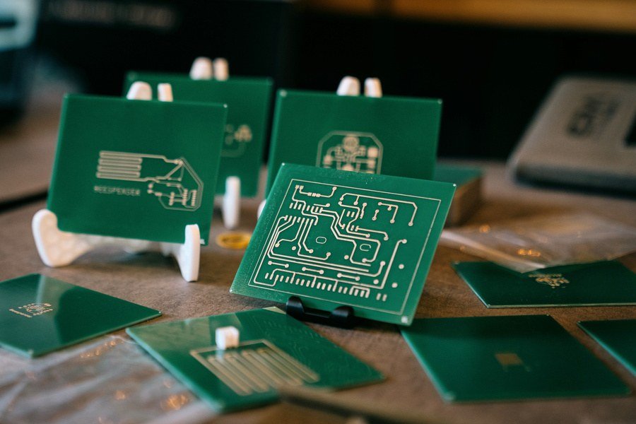
Printed double-sided PCB boards
ELECTRONICS & CIRCUITS

Double-sided PCB on FR4

Front and back circuit layers on 1.6 mm FR4, with drilling and second-side alignment in one workflow.

VIEW APPLICATION
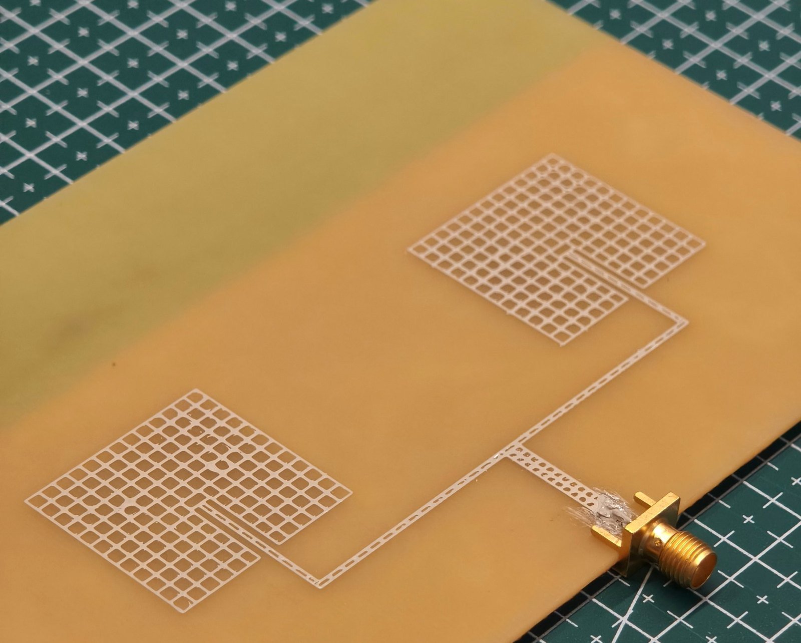
Printed RF antenna on FR4 with SMA connector
RF & ANTENNAS

Printed RF antennas

One antenna geometry on FR4 and on PET bonded to glass, compared with VNA reflection measurements.

VIEW APPLICATION
Printed electrochemical electrodes on clear film
SENSORS

Biosensor electrodes

Three-electrode patterns printed in silver and carbon BeeInk as one multilayer structure.

VIEW APPLICATION
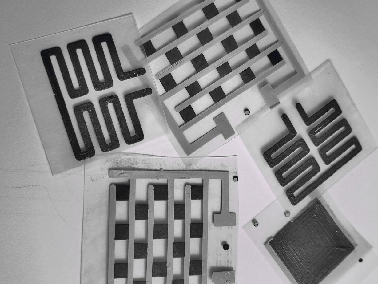
Printed carbon strain gauge patterns
SENSORS

Strain gauge patterns

Four carbon meander structures on flexible film, with features measured down to 127.85 µm.

VIEW APPLICATION
Printed membrane switch circuit on flexible film
INTERFACES

Membrane switch circuits

Silver circuit and carbon contact layers printed on PET for flexible user interfaces.

VIEW APPLICATION
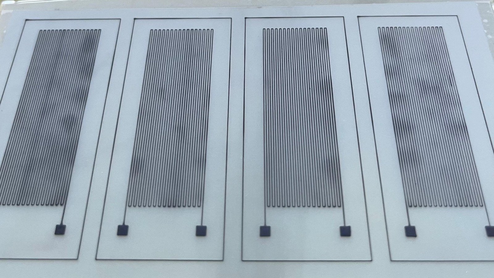
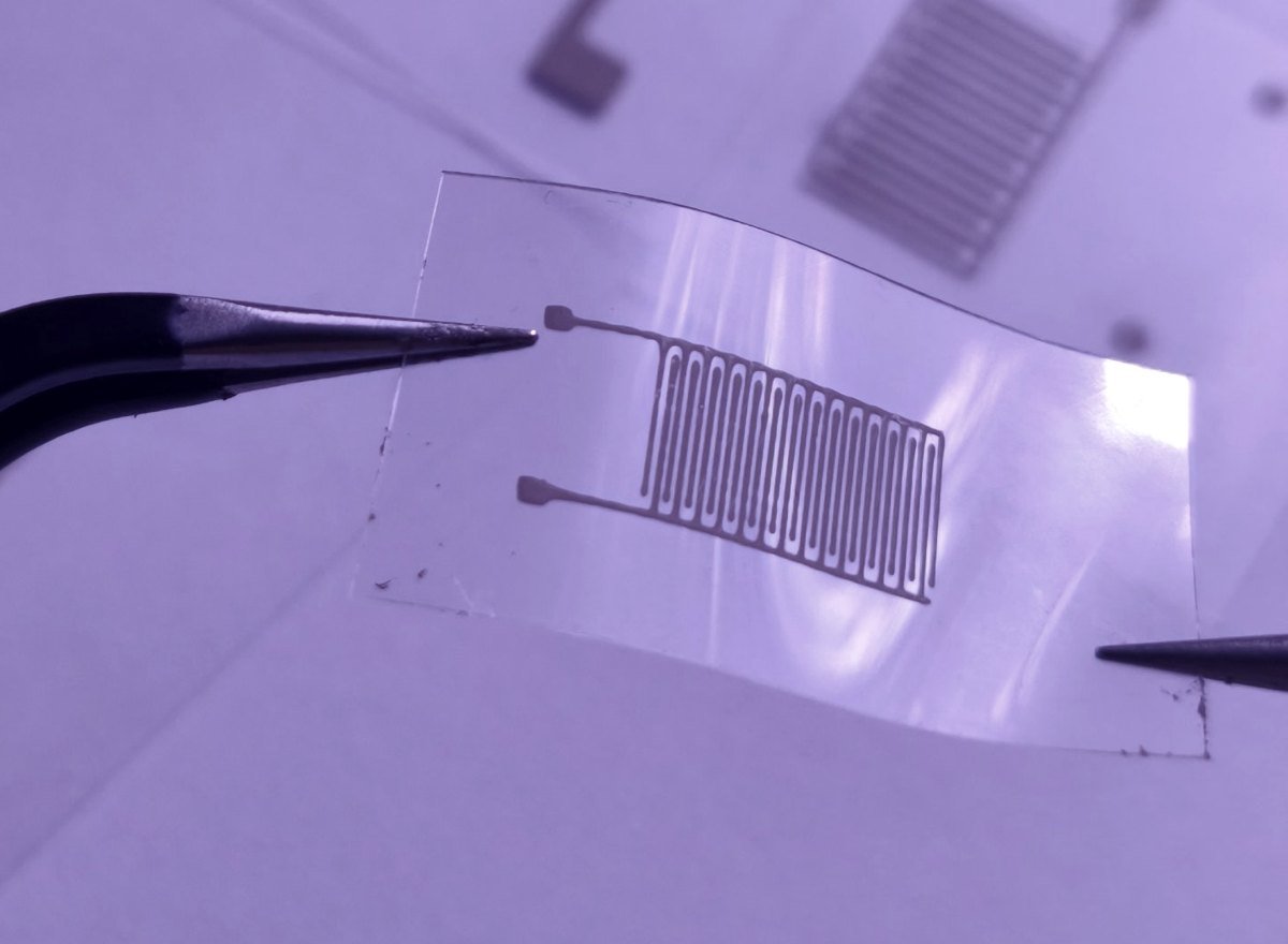
Printed silver interdigitated electrodes on PET
SENSORS

Interdigitated electrodes

Silver fingers 200 µm wide with 200 µm gaps, printed on flexible PET.

VIEW APPLICATION
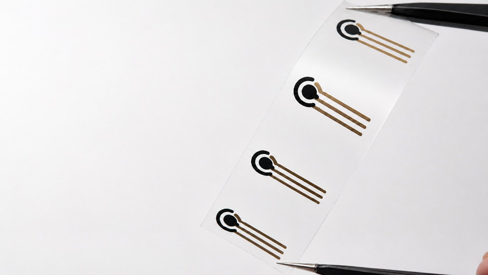
Flexible printed heaters on PET
HEATERS

Flexible heaters

Two silver and carbon heater architectures on 125 µm PET, reaching 180 °C.

VIEW APPLICATION
Explore all applications VIEW ALL
MATERIALS

Use the material your work requires.

BEEINKDEVELOPED AND PRODUCED BY BEESPENSER
MATERIAL FAMILYKEY CHARACTERISTICTYPICAL APPLICATIONS
01Silver-based inkBEEINKHigh conductivityCircuits, heaters, antennas
02Graphene-based inkBEEINKResistive and electrochemical functionalitySensors, electrodes
03Carbon black inkFunctional conductive networksSensors, energy devices
04Stretchable silver inkConductivity under deformationWearables, soft electronics
05Dielectric inkElectrical insulation and layer separationMultilayer circuits, crossovers, encapsulation, insulation layers
06Battery materialsElectrode and electrolyte prototypingBatteries, supercapacitors
07Your own formulation1,000 – 100,000 cP viscosity rangeIn-house materials research

Working with a material that is not listed here? Talk to us.

EXPLORE MATERIALS


Trusted by research labs and institutions.

TÜBİTAK UME
İstanbul Üniversitesi-Cerrahpaşa Nanoteknoloji ve Biyoteknoloji Enstitüsü
Bilkent University UNAM
Erciyes Üniversitesi
İTÜ Çekirdek Incubation Center
Sabancı Arf
Istanbul Okan University
Özel SANKO Okulları
TÜBİTAK UME
İstanbul Üniversitesi-Cerrahpaşa Nanoteknoloji ve Biyoteknoloji Enstitüsü
Bilkent University UNAM
Erciyes Üniversitesi
İTÜ Çekirdek Incubation Center
Sabancı Arf
Istanbul Okan University
Özel SANKO Okulları
TÜBİTAK UME
İstanbul Üniversitesi-Cerrahpaşa Nanoteknoloji ve Biyoteknoloji Enstitüsü
Bilkent University UNAM
Erciyes Üniversitesi
İTÜ Çekirdek Incubation Center
Sabancı Arf
Istanbul Okan University
Özel SANKO Okulları

Our supporters.

TÜBİTAK
Türkiye Kalkınma Fonu
Sabancı Arf
EIT Manufacturing, co-funded by the European Union
İTÜ ARI Teknokent
YES!Delft
SPIN SUNUM
TÜBİTAK
Türkiye Kalkınma Fonu
Sabancı Arf
EIT Manufacturing, co-funded by the European Union
İTÜ ARI Teknokent
YES!Delft
SPIN SUNUM
TÜBİTAK
Türkiye Kalkınma Fonu
Sabancı Arf
EIT Manufacturing, co-funded by the European Union
İTÜ ARI Teknokent
YES!Delft
SPIN SUNUM

What will you print next?

Get a Quote Book a Demo EXPLORE APPLICATIONS