How precisely can fine conductive lines be printed, and how consistently?
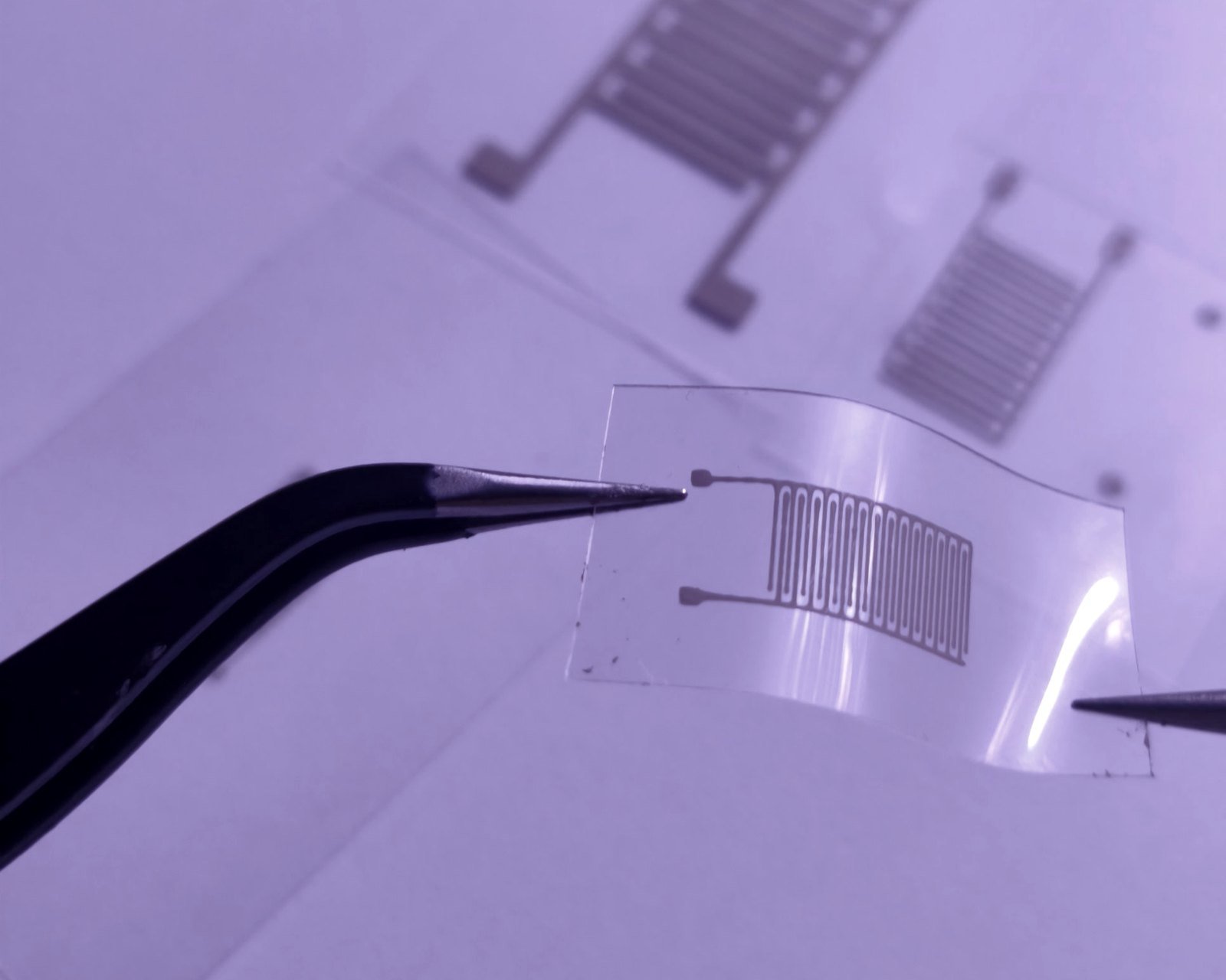
In this study, interdigitated electrode (IDE) structures were printed on PET using silver conductive ink and Beespenser's Monobee microdispensing platform, then thermally cured at 150 °C for 15 minutes.
Rather than developing a complete sensor, the study focused on an essential step in printed electronics research: establishing the feasibility of fabricating fine, closely spaced conductive patterns.
Purpose
Interdigitated electrodes are widely used in sensor research, dielectric characterization and other applications that need closely spaced conductive structures. Their geometry of alternating fingers separated by narrow gaps means the dimensions and consistency of each feature influence the electrical behavior of the whole structure.
The purpose of this study was to investigate Monobee's ability to print fine silver lines on a flexible PET substrate while keeping the pattern consistent. The structures were produced as fabrication test samples, without integration into a complete sensing device.
Fine-line printing
Exploring the minimum achievable trace width under the selected printing conditions.
Pattern consistency
Observing the continuity, definition and uniformity of the printed paths throughout the IDE geometry.
A compact test for printing precision.
The alternating finger arrangement means many narrow features must be deposited close to one another while keeping their intended geometry. That makes IDEs a demanding, practical test of a fine-line printing process.
Beyond fabrication studies, IDE structures can become the base of capacitive, impedance-based and functional sensors when combined with suitable materials and measurement systems.
Fabricating silver IDEs with Monobee
The electrodes were fabricated with Monobee's Direct Ink Writing process: silver conductive ink was deposited onto PET along the digitally defined electrode pattern.
Materials and processing
| Printing platform | Monobee |
| Printing technology | Direct Ink Writing (DIW) |
| Electrode material | Silver conductive ink |
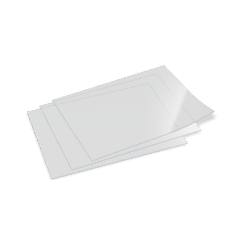
| Substrate | PET (polyethylene terephthalate) |
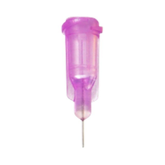
| Tip | 30G metal syringe tip, 0.16 mm ID |
| Printed structure | Interdigitated electrodes |
| Finger width | 200 µm |
| Gap between fingers | 200 µm |
| Finger length | 5.4 mm |
| Curing | 150 °C · 15 minutes |
| Evaluation focus | Fine-line printing and pattern consistency |
Fabrication workflow
- 01Electrode designAn IDE pattern was prepared with closely spaced fingers to investigate fine-line printing behavior.
- 02Silver ink depositionThe electrode geometry was printed directly onto PET by controlled microdispensing.
- 03Thermal curingThe printed silver structures were cured at 150 °C for 15 minutes.
- 04Pattern evaluationThe electrodes were examined for fine-line definition and the consistency of printed paths.
Consumables
Printing results and observations
Fine-line printing. Monobee printed silver fingers 200 µm wide, separated by 200 µm gaps, along a 5.4 mm finger length. The study also helped identify the practical limits of the tested printing conditions.
Consistency across features. The printed samples showed consistent line formation across the IDE pattern, supporting the feasibility of producing closely spaced silver features with Monobee.
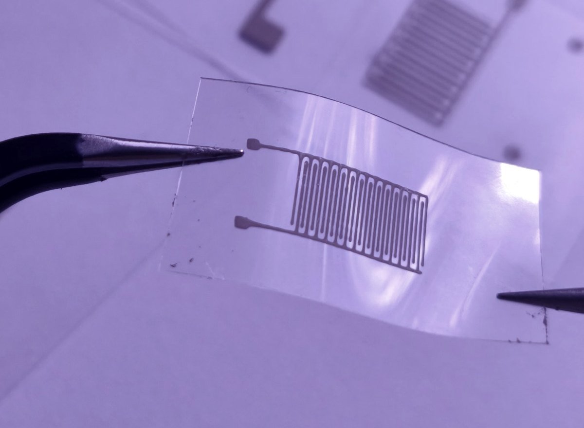
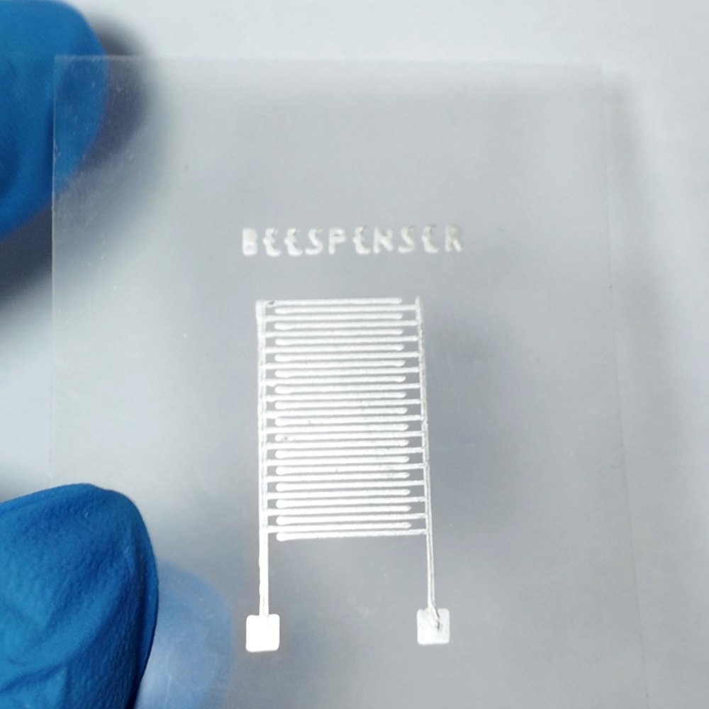
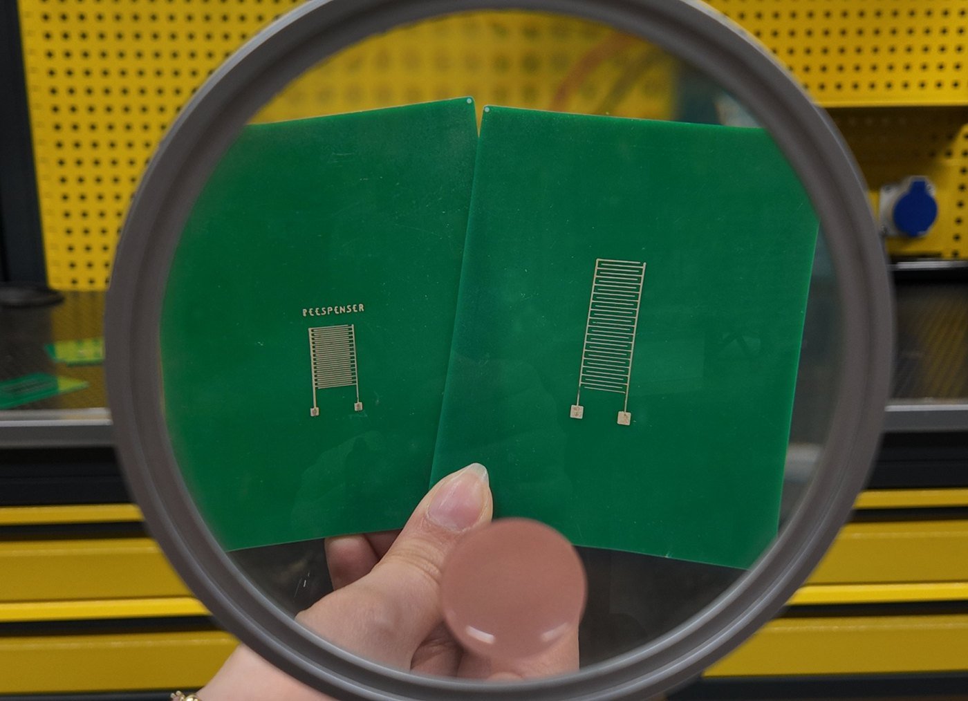
These observations relate to the printed geometry. Long-term electrical stability and sensing performance were not evaluated in this study.
Fine-line printing is not only about how narrow a single trace can be. It is about keeping every feature consistent throughout the design.
IDEs are a useful test structure because printing performance is judged across many adjacent fingers, not an isolated line. For researchers developing printed electrodes, reliable pattern formation is the step that comes before adding sensing materials or moving to functional device testing.
Why prototype IDEs with Monobee?
Direct Ink Writing deposits conductive patterns straight from a digital design. Researchers can explore new electrode geometries, printing parameters and compatible materials in-house, before committing to more complex device development.
Potential applications
This study focused on printing performance, but IDE structures are relevant to several research fields.
- Capacitive and impedance sensors Electrical responses linked to changes in capacitance and impedance.
- Humidity and gas sensing With a suitable sensing layer, IDEs can respond to environmental or chemical changes.
- Material characterization Dielectric properties, functional coatings and electrical response of deposited materials.
- Lab-on-chip and liquid analysis Compact electrodes inside platforms for studying liquids and material interactions.
- Flexible sensor research Electrode structures on flexible substrates for conformable and wearable devices.
These are potential research applications of IDE technology. They were not experimentally demonstrated as complete devices in this study.
A defined geometry is the best test of precision.
By focusing on fine-line deposition and the consistency of closely spaced conductive paths, this study gave practical insight into Monobee’s capabilities for printed electrode prototyping, and a base for further development of functional printed electronics.
RELATED MATERIALS: SILVER CONDUCTIVE INKS →Their closely spaced finger geometry makes them useful for evaluating fine conductive lines and pattern consistency.