FRONT SIDE
Front-side circuit
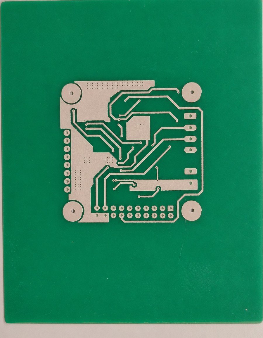
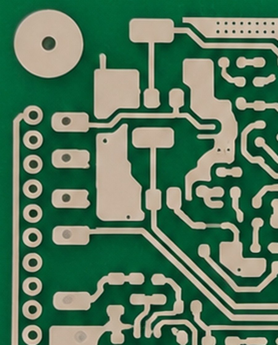
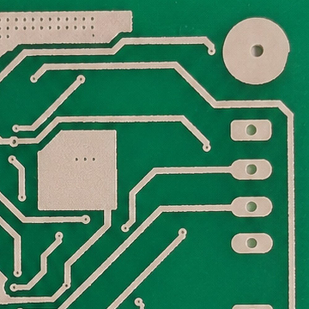
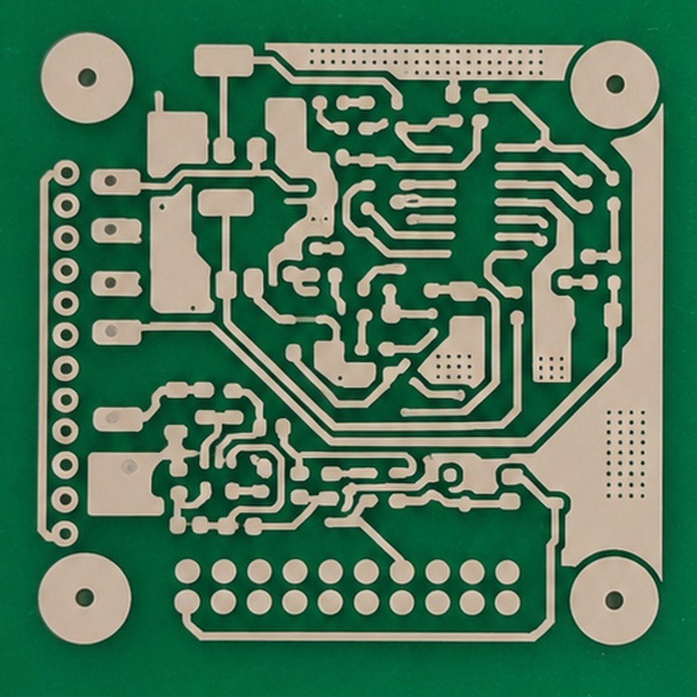
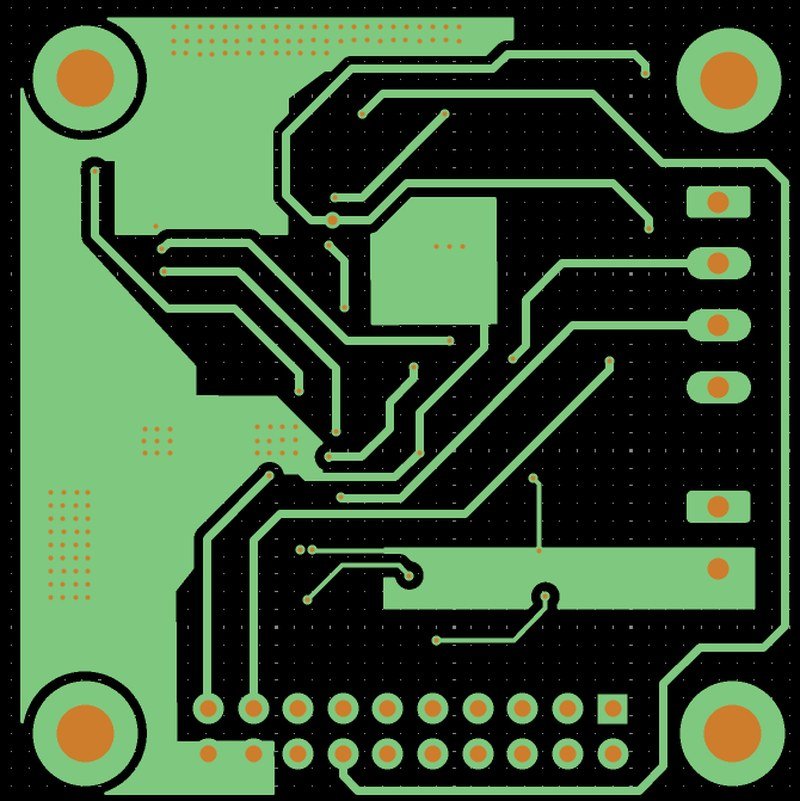
A denser arrangement of conductive traces, connection pads and component mounting regions, printed on the first face of the board.
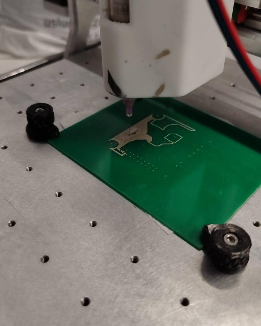
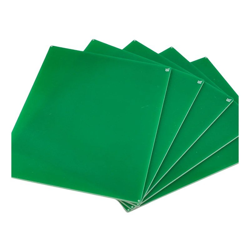
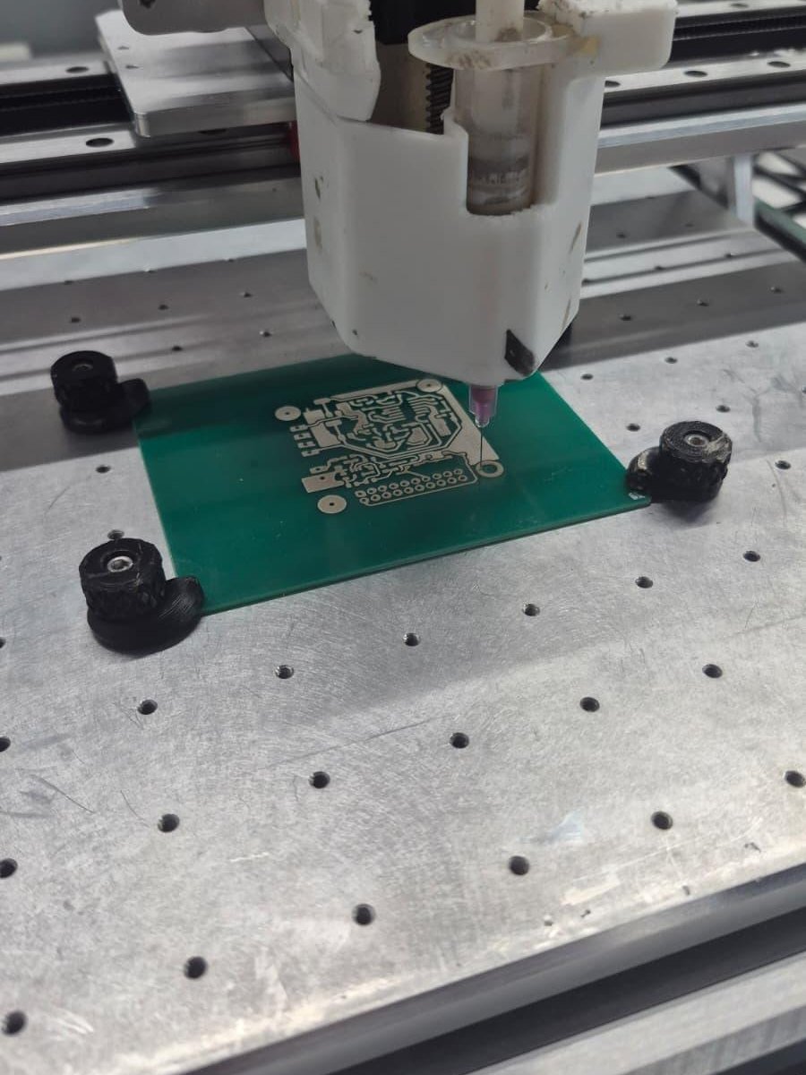
A double-sided motor driver PCB prototype was printed with Monobee on 1.6 mm FR4, using silver nanoparticle-based conductive ink and a 160 µm metal nozzle.
Surface calibration, drilling, conductive pattern deposition and second-side alignment were brought together in a single in-house prototyping workflow.
Custom electronic circuits often go through several iterations before a design is ready for manufacturing. For low-volume prototypes, outsourced PCB fabrication adds cost, delivery time and operational steps to every iteration.
In this demonstration, Monobee fabricated a double-sided motor driver PCB prototype developed as part of the EmbedTech project. The front- and back-side layouts were prepared digitally and transferred onto FR4 with silver nanoparticle-based conductive ink.
The objective was to show a practical way to produce custom, low-volume circuit prototypes in-house.
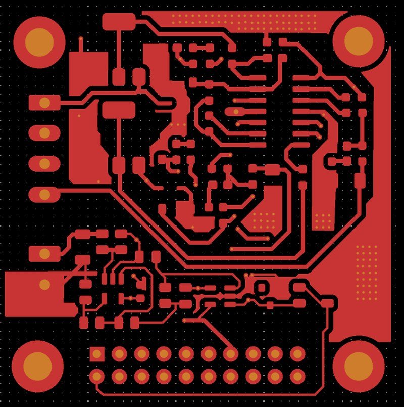
The motor driver PCB distributes its conductive patterns across both faces of the FR4 board. Each side was prepared as its own layer in the digital design and printed to its own geometry.
Accurate positioning keeps the intended relationship between the two printed patterns and the drilled hole locations.
A denser arrangement of conductive traces, connection pads and component mounting regions, printed on the first face of the board.
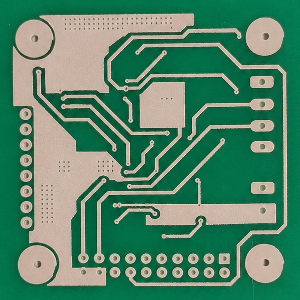
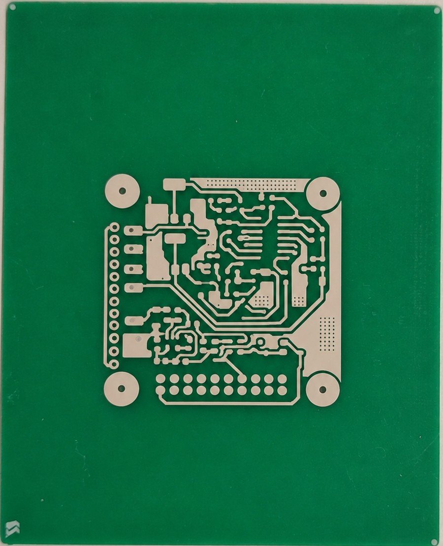
Additional routing that completes the circuit layout. The board was repositioned and the second-side geometry aligned with the physical substrate before printing.
The Drilling Module prepared the holes defined in the PCB design, including component, mounting and interconnection locations.
The prototype was produced through four documented operations, all run on Monobee. Together they took approximately 4 hours and 25 minutes.
| PARAMETER | VALUE |
|---|---|
| Substrate | FR4 |
| Substrate thickness | 1.6 mm |
| Conductive material | Silver nanoparticle-based ink |
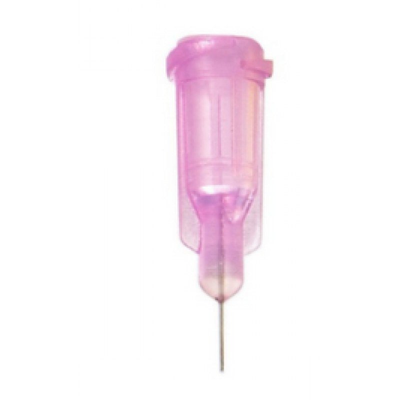
| Tip | 30G metal syringe tip, 160 µm inner diameter |
| PCB architecture | Double-sided |
| Production time | ≈ 4 h 25 min |
Printing one surface is only part of a double-sided board. Once the substrate is turned over, the second design has to be positioned relative to the physical board and the features already in place.
Here, the back-side geometry was aligned after the FR4 board was repositioned. Monobee's digital workflow handled surface calibration, print positioning, nozzle-height adjustment and preparation of the second print.
Traces, pads and drilled holes on both faces have to keep their positional relationship. Running these steps on one platform makes two-sided PCB designs practical to explore during early-stage prototyping.
The demonstration produced a physical double-sided PCB prototype whose conductive patterns follow the prepared front- and back-side layouts. Both printed surfaces were documented and compared visually with their digital designs.
This work establishes fabrication feasibility. Electrical continuity, component-level operation and complete motor-driver functionality call for additional documented testing.
Double-sided prototyping is more than printing twice.
The substrate has to be positioned, drilled, calibrated and repositioned while the intended relationship between the circuit layers is kept. In this demonstration, those operations ran as one connected Monobee workflow.
For research teams and product developers, this shows how additive deposition and integrated drilling can be combined to explore custom PCB designs in-house, faster and more cost-efficiently, without a separate fabrication run for every iteration.
More flexibility during circuit development.
Monobee printed a double-sided motor driver PCB prototype on 1.6 mm FR4 in about 4 hours and 25 minutes, combining surface calibration, drilling, conductive deposition and second-side alignment in one in-house workflow.
RELATED MATERIALS: SILVER CONDUCTIVE INKS →Yes. This demonstration documents front- and back-side conductive PCB patterns printed on a 1.6 mm FR4 substrate.